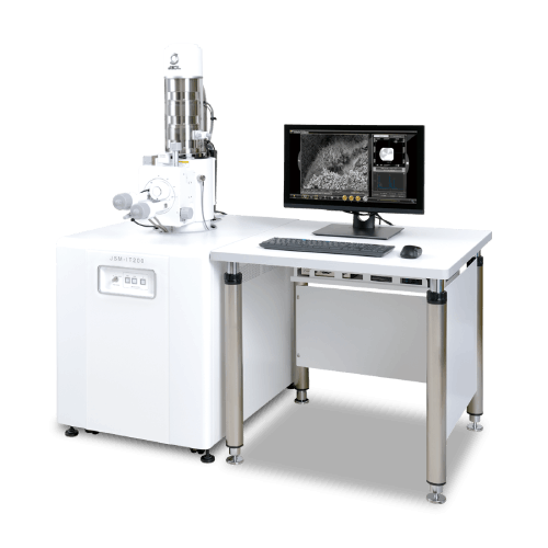
Scanning Electron Microscope

The Scanning Electron Microscope (SEM) is an important tool in the field of research and image analysis. The primary function of SEM is to create detailed images of materials at the micro and nanoscale by utilizing an electron beam to scan the sample. Here are some important functions of SEM:
– Detailed imaging with high magnification.
– Analysis of shape and size.
– Determination of chemical composition.
– Study of material structure.
– Applications in science and industry.
– Capability for 3D imaging.

  • Model: JSM-IT200
  • Manufacturer: Jeol
  • Origin: Japan

Description

Accelerating Voltage:
– 53 steps
– 0.5 to 3 kV: Variable in 100 V steps
– 3 to 30 kV: Variable in 1 kV step
– Resolution:
High vacuum mode
Secondary electron image (SEI)
+ 3.0 nm (Acc. V 30 kV, 8mm WD)
+ 8.0 nm (Acc. V 3 kV, 6mm WD)
+ 15.0 nm (Acc. V 1 kV, 6mm WD)
Low vacuum mode:
Backscattered electron image (BEI):
– 4.0 nm (Acc. V 30 kV, 5mm WD)
– Signal:
High-vacuum mode
+ SEI (E.T. detector)
+ BEI (composition, topographic and stereoscopic images by semiconductor detector)
Low-vacuum mode
+ BEI (composition, topographic and stereoscopic images by semiconductor detector)
– Magnification
+ Screen magnification: ×14 to ×839,724 (Magnification defined with the display size 358 mm × 269 mm)
– Probe current: 1 pA to l µA when using the movable aperture
– Pressure range: 10 to 100 Pa

If you have extra question or have some projects having this product, please feel free to reach out to us!

Reviews

There are no reviews yet.

Be the first to review “Scanning Electron Microscope”

Your email address will not be published. Required fields are marked *

Go to Top